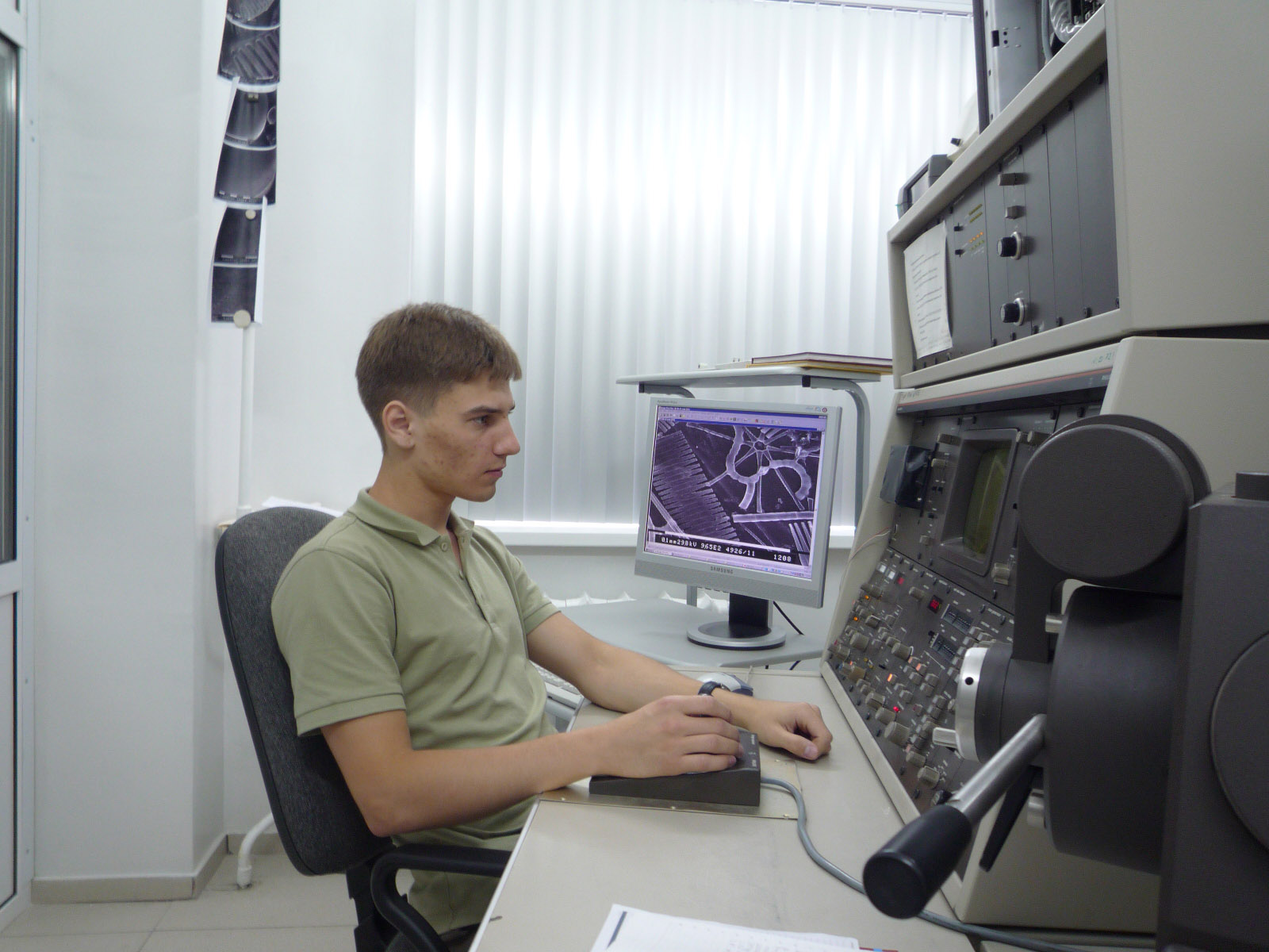
Philips' SEM 525-M provides all the facilities needed for fast, nondestructive inspection of large samples.
Detailed information can be obtained from specimens up to 200mm (8") in diameter, thanks to the microscope's combination of extensive specimen manoeuvrability and high resolution imaging at all specimen orientations. Complementary information from each point of interest can be gathered simultaneously by the microscope's multiple detectors, and straightforward system set-un is assured even for the most challenging applications.
The remarkable capabilities of the SEM 525-M are the result of designing the instrument specifically to meet the demands of microscopists working principally with large specimens; for example, semiconductor wafers up to 8" in diameter, or the bulky specimens often encountered in mechanical engineering applications and forensic science. Operations that are normally time-consuming, such as relocating areas of interest, focussing, astigmatism correction, or selection of detectors, can all be executed quickly by simple pushbutton operations.
In routine yet demanding industrial applications such as IC linewidth measurement, the SEM 525-M can save time and increase the reliability of results through automation of sophisticated inspection procedures. This is made possible by the microscope's built-in data link, which permits an external computer to control major operating parameters remotely.